
丨
Views: 0 Author: Site Editor Publish Time: 2026-10-09 Origin: Site


Modern wireless, telecom, and radar systems rely heavily on precise signal management. The Time Division Duplexing (TDD) RF Power Amplifier is a critical component in these advanced architectures. It allows transmit (Tx) and receive (Rx) functions to share the exact same frequency band. It achieves this through rapid time-slot switching. We wrote this guide for engineers and procurement teams evaluating components for system integration. Moving from basic theory to operational reality is essential for project success.
You must constantly balance competing hardware demands. Output power, thermal management, and signal linearity often clash with unit cost and system footprint limits. Understanding how these amplifiers operate helps you make better design choices. In this article, we explore the fundamental mechanics of TDD systems. We examine common integration challenges you will face. Finally, we provide a comprehensive framework to help you evaluate and select the right amplifier components for your specific operational requirements.
Switching Speed is Critical: TDD operations require precise microsecond switching between Tx and Rx modes to prevent signal collision and receiver damage.
Efficiency Requires Correction: Techniques like Digital Pre-Distortion (DPD) are standard for maximizing efficiency without sacrificing linearity in modern modules.
Scalability Matches Application: Selection hinges on matching power requirements—such as a 20W TDD Integrated Power Amplifier for localized networks vs. a 50W TDD RF Power Amplifier for macro-cell or defense applications.
Integration Mitigates Risk: Choosing a pre-matched, integrated TDD RF Power Amplifier Module reduces bias circuit design risks and accelerates time-to-market.
To understand system performance, we first need to look at how a TDD RF Power Amplifier actually functions. It operates very differently from traditional Frequency Division Duplexing (FDD) setups. Both methods handle two-way communication, but they route signals using distinct physical principles.
TDD isolates the transmit and receive paths in the time domain. It does not separate them in the frequency domain. FDD requires two separate frequency bands. It also relies on bulky hardware duplexers to keep high-power transmit signals from destroying sensitive receive circuits. TDD eliminates these heavy duplexers completely. Both upstream and downstream traffic share one frequency band. They take turns using the channel.
This approach saves enormous physical space. However, it demands high-speed synchronization. The system must coordinate exact timing between the base station and the user equipment. If the transmitter stays on a microsecond too long, it will collide with incoming receive signals. You lose data, and you risk damaging the hardware.
Feature | Time Division Duplexing (TDD) | Frequency Division Duplexing (FDD) |
|---|---|---|
Duplexing Method | Time-slot separation | Frequency band separation |
Hardware Footprint | Compact (no large duplexers needed) | Large (requires bulky cavity duplexers) |
Spectrum Efficiency | Highly efficient for asymmetric data loads | Requires paired spectrum blocks |
Synchronization | Requires precise network-wide timing | Minimal timing coordination required |
The internal signal path of these amplifiers requires careful engineering. The journey begins at the baseband input. Low-power RF signals enter the module. They travel through early driver stages. These drivers step up the gain cleanly. Finally, the signal hits the main power amplification stage. Here, high-power transistors (often GaN or LDMOS) boost the signal to its final output level.
High-speed RF switches direct this traffic flow. You will typically see circulators, isolators, or solid-state switches built into the module. Solid-state switches, like PIN diodes or specialized FETs, act as traffic cops. They toggle the antenna connection between the Tx power stage and the Rx low-noise stage. They must isolate the two paths completely.
Engineers must decide how to trigger these rapid Tx/Rx transitions. There are two primary control methods used in modern designs:
Manual/External Pin Switching: This method requires an external baseband control signal. The processor sends a distinct logic high or low to a control pin. It tells the amplifier exactly when to switch states. It is highly reliable. However, it relies heavily on your system having perfect timing accuracy. If your software lags, your hardware suffers.
Auto-Switching: This method senses inbound RF power directly. When it detects an active transmit signal, it toggles the state automatically. It reduces control overhead significantly. You do not need to route complex timing traces across your board. However, it introduces slight latency considerations. The sensor needs a tiny fraction of a microsecond to react.
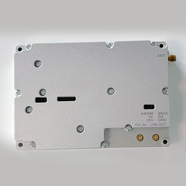
Integrating high-frequency components is rarely simple. TDD systems bring their own unique set of engineering hurdles. When you switch high power loads on and off millions of times a second, physical limits get tested. We see three major challenges repeatedly in field integrations.
Managing dynamic bias circuits is a severe engineering challenge. The amplifier stages cannot remain fully powered during the receive cycle. Leaving them on wastes energy and generates excess thermal noise. This noise degrades the sensitive receiver.
Therefore, the bias circuit must turn the main power transistors on and off rapidly. We call this gate switching or drain modulation. Designing a circuit that powers up a high-current transistor in nanoseconds without causing voltage spikes is difficult. Poor bias design leads to ringing, oscillation, or sluggish turn-on times. This cuts into the usable data transmission window.
Heat kills electronics. In telecom and radar systems, we deal with complex modulation schemes like Orthogonal Frequency Division Multiplexing (OFDM). These schemes have very high Peak-to-Average Power Ratios (PAPR).
High PAPR means the signal occasionally spikes to massive power levels, even if the average power is low. These spikes create intense, localized heat spots on the semiconductor die. Because a TDD system pulses on and off, the hardware undergoes continuous thermal cycling. Over time, expansion and contraction cause mechanical stress. You need robust heat sinking. You must spread this thermal energy quickly to maintain long-term reliability.
Sudden state changes cause signal distortion. When you blast high power loads through a transistor, it behaves non-linearly near its peak limits. The output no longer perfectly matches the input shape.
Memory effects make this worse. A transistor's behavior at any given microsecond depends partly on what it did a microsecond ago. Trapped charges in the semiconductor and localized thermal shifts cause lag. This distortion threatens regulatory emission compliance. If your signal spills into adjacent frequency bands, you violate FCC or CE rules. It also corrupts your own signal, severely reducing system data throughput.
Procurement teams and lead engineers must bridge the gap between technical specs and application needs. You want to buy exactly what your system requires. Over-prescribing specs wastes money. Under-prescribing causes system failure in the field.
You must connect specific power levels directly to your use cases. Different deployment environments dictate different hardware choices.
A 20W TDD Integrated Power Amplifier is highly versatile. It is ideal for small cells in urban environments. We also see it heavily used in Unmanned Aerial Systems (UAS) communication links and private campus networks. In these applications, SWaP (Size, Weight, and Power) constraints are rigorous. You need enough power to push through light foliage and rain, but you cannot drain a drone battery or overheat a pole-mounted enclosure.
Conversely, a 50W TDD RF Power Amplifier serves much larger environments. It is perfectly suited for macro base stations. Wide-area tactical communications and electronic warfare (EW) systems also rely on this power class. When range and obstacle penetration dictate higher output, 50 watts provides the necessary punch. However, it requires a dramatically different thermal management strategy.
Hardware alone cannot achieve maximum efficiency while maintaining linearity. Digital Pre-Distortion (DPD) algorithms are critical. DPD acts as an intelligent software layer. It predicts how the amplifier will distort the signal.
It then creates an exact inverse of that distortion and applies it to the signal before it enters the amplifier. When this pre-distorted signal hits the non-linear hardware, the two effects cancel out. The final output is incredibly clean. DPD allows the hardware to run much closer to saturation. Saturation is where the amplifier achieves its maximum electrical efficiency. Without DPD, you would have to back off the power significantly to stay compliant.
You face a "build vs. buy" decision when integrating RF stages. Discrete component design involves buying raw transistors, capacitors, and switches. You must design the matching networks and bias circuits yourself. This carries high engineering overhead. It requires specialized RF engineers and months of tuning.
Alternatively, utilizing a fully characterized TDD RF Power Amplifier Module changes the equation. A module is a pre-packaged solution. The manufacturer has already done the impedance matching. They have integrated the bias controllers. This provides predictable integration and guaranteed performance specifications. It drastically accelerates your product's time-to-market.
How do you sort through vendor datasheets? You need a structured decision framework. Not all specifications carry the same weight. Focus on the metrics that directly impact your deployment success.
When reviewing technical data, demand clarity on these three parameters:
Tx/Rx Switching Time: This metric must align perfectly with your baseband processing capabilities. Modern systems require sub-microsecond switching. If the amplifier takes too long to toggle, you will drop data packets.
Gain Flatness & Linearity: Check the gain response across your entire operational bandwidth. The gain should not spike or dip unpredictably. Flat gain ensures uniform signal strength across all channels.
Isolation Metrics: High isolation is non-negotiable. The RF switch must completely block the high-power transmit signal from bleeding back into the receive path. Poor isolation will destroy sensitive Low Noise Amplifiers (LNAs) instantly.
Never trust top-line marketing numbers blindly. Require comprehensive testing data from your vendors. Look for manufacturers who provide clear S-parameters. S-parameters show exactly how the module behaves at specific frequencies.
Furthermore, demand thermal derating curves. A component might produce 50 watts at room temperature, but what happens at 85 degrees Celsius? You need realistic Mean Time Between Failures (MTBF) calculations. Crucially, these calculations must be performed under actual TDD duty cycles. Many vendors only test under Continuous Wave (CW) benchmarks. CW testing does not reflect the aggressive thermal cycling of real TDD operations.
Hardware must survive its environment. Ensure the component meets the necessary industrial standards. If you are building defense or aerospace equipment, look for MIL-STD environmental compliances for shock, vibration, and extreme temperatures.
Finally, evaluate the vendor's long-term supply stability. RF components undergo frequent lifecycle changes. You do not want to design your entire base station around a module that gets discontinued in twelve months. Ask about long-term production guarantees.
Selecting a TDD RF Power Amplifier is rarely just about chasing raw power. It requires managing the operational complexities of rapid switching, heavy thermal loads, and stringent signal integrity. FDD architectures use space and filters to solve problems. TDD architectures rely on precision timing and robust solid-state engineering.
Your next step is to document your precise system parameters. Define your exact duty cycles. Map out your peak power requirements and identify your strict footprint limits. Armed with this data, you can begin matching your needs with manufacturer specification sheets confidently. If standard modules do not fit, use these metrics to request targeted custom engineering consultations from trusted vendors.
A: The necessary switching speed usually falls in the range of nanoseconds to a few microseconds. The exact requirement depends entirely on your specific protocol. Technologies like 5G NR and modern Wi-Fi demand extremely tight timing. Custom tactical waveforms might vary, but sub-microsecond transition times are generally the industry standard to prevent packet loss.
A: Modules provide pre-matched impedance, fully integrated biasing, and defined thermal interfaces. Designing discrete RF matching networks requires extensive trial and error. By choosing a pre-packaged module, you significantly reduce engineering risk, cut down on debugging time, and drastically accelerate your product development cycles.
A: The duty cycle dictates the true average power dissipation. If you have a 50W peak amplifier operating at a 20% Tx duty cycle, it only outputs 10W of average power. This fundamentally changes the necessary thermal management strategy. You can use smaller heat sinks compared to a system running in continuous operation.
A: No. DPD highly mitigates distortion to acceptable regulatory levels, but it cannot perform miracles. The inherent physical limitations of the semiconductor material (whether GaN, LDMOS, or GaAs) still define the absolute boundaries of operation. DPD simply allows you to push the hardware much closer to those boundaries safely.


