
丨
Views: 0 Author: Site Editor Publish Time: 2026-10-16 Origin: Site


The shift toward private 5G and LTE networks is fundamentally reshaping industrial connectivity across the globe. Organizations increasingly deploy custom networks utilizing spectrums like CBRS or Band n77/n78 to guarantee secure, high-bandwidth communication. This transformation introduces a critical bottleneck: precise RF hardware selection. At the heart of this hardware challenge lies the amplifier stage. Power Amplifiers ultimately dictate total system energy consumption, stringent thermal management needs, and the overall network coverage footprint. A poorly chosen component can easily jeopardize your entire wireless infrastructure. This guide provides network architects and RF engineers with a practical, evidence-based evaluation framework. We explore how to assess essential switching speeds, cutting-edge material advantages, and rigorous testing protocols. You will learn exactly how to shortlist TDD-specific components effectively for your next mission-critical deployment.
TDD architectures demand precise switching speeds; inadequate PA switching leads to packet loss and spectral overlap.
Evaluating a Wireless Communication Power Amplifier requires balancing Power Added Efficiency (PAE) with strict linearity (ACLR/EVM) requirements.
GaN TDD Power Amplifiers have become the baseline for modern private networks due to superior thermal performance and wideband capabilities compared to legacy LDMOS.
Implementation success relies heavily on testing the PA alongside your intended Digital Pre-Distortion (DPD) algorithms.
Time Division Duplexing (TDD) fundamentally changes how base station amplifiers operate. In standard Frequency Division Duplexing (FDD), the amplifier remains continuously active on a dedicated frequency. It operates in a steady thermal state. TDD, however, uses a single frequency band. It relies on rapidly alternating time slots for uplink and downlink traffic. This mechanism forces the amplifier to rapidly pulse on and off.
This rapid cycling exposes the hardware to severe thermal stress. The silicon or gallium nitride junctions heat up during transmission bursts. They cool down during reception slots. These constant micro-fluctuations create intense mechanical stress on wire bonds and die attach materials. Furthermore, switching transients introduce electrical noise. Standard continuous-wave devices simply cannot survive this punishing environment without degrading quickly.
Private wireless networks rarely mimic standard consumer network profiles. Consumer networks are heavily downlink-oriented. Users stream video or download files. Private networks often require custom configurations tailored for industrial tasks. These tasks demand higher uplink ratios.
Video Surveillance: Security systems push continuous, high-resolution video streams back to central servers.
Industrial IoT: Thousands of sensors transmit continuous telemetry, vibration, and temperature data.
Automated Guided Vehicles (AGVs): Warehouse robots require constant positional uplink updates to prevent collisions.
These uplink-heavy ratios increase the sustained thermal load on the amplifier. The component spends significantly more time transmitting. It generates massive amounts of heat over prolonged periods. Selecting an amplifier built natively for TDD environments becomes absolutely crucial. It prevents premature hardware degradation. It also ensures reliable, ultra-low latency performance for your mission-critical applications.
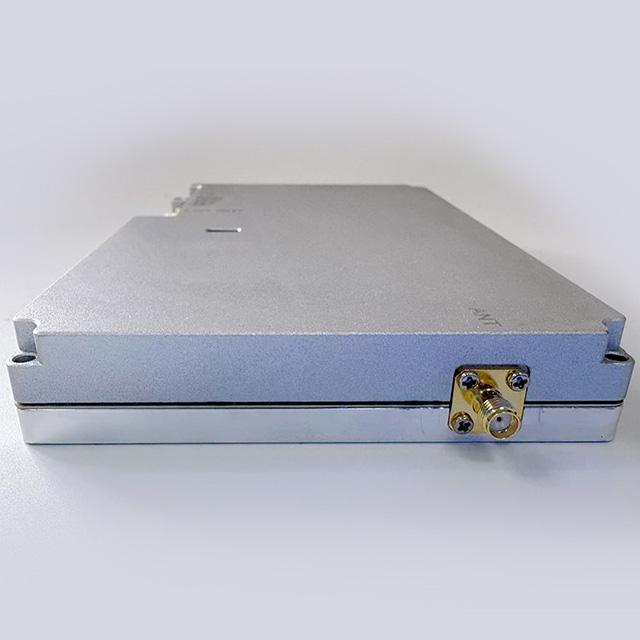
Evaluating modern RF hardware requires a deep understanding of competing metrics. You cannot optimize every parameter simultaneously. Engineers must balance these specifications based on the desired network outcome.
Linearity and efficiency represent the most critical engineering trade-off. You must maintain low Error Vector Magnitude (EVM) and Adjacent Channel Leakage Ratio (ACLR). EVM measures modulation accuracy. Poor EVM forces the network to drop from high-order modulation schemes, like 256-QAM, down to slower schemes like 64-QAM. This drop severely throttles data throughput.
ACLR measures how much energy leaks into neighboring frequency bands. Strict regulatory frameworks, like FCC Part 96 for CBRS, mandate pristine spectrum usage. Spectral splatter leads to immediate regulatory compliance failures. You must prioritize linearity to maintain network legality and signal clarity.
At the same time, Power Added Efficiency (PAE) directly influences operational expenses. PAE measures how effectively the amplifier converts DC power into usable RF energy. High PAE reduces the physical cooling requirements. It allows for a noticeably smaller base station footprint. Finding the optimal sweet spot between clean linearity and high PAE defines a successful component selection.
You must rigorously evaluate TDD switching latency. Look closely at the integration of internal RF switches and bias control circuits. The amplifier must power up, stabilize, and power down within mere microseconds. The 5G New Radio (NR) standard relies on highly precise slot formats.
Slow switching times will inevitably corrupt physical layer framing. If the amplifier powers down too slowly, it transmits energy into the receiving time slot. This causes spectral overlap. It creates self-interference, dropping packets and spiking network latency. Fast, precise switching control is non-negotiable.
Finally, prioritize gain flatness across the entire operating bandwidth. Modern private networks utilize increasingly wide bandwidths. Sub-6GHz bands often span 100MHz or more continuously. The amplifier must provide consistent gain across this entire spectrum. If the gain rolls off at the band edges, the outer subcarriers will suffer from poor signal-to-noise ratios. Consistent performance ensures stable data throughput across the entire channel.
The RF industry has largely shifted semiconductor materials to meet rigorous 5G demands. Traditional Laterally Diffused Metal Oxide Semiconductor (LDMOS) technologies face severe physical limitations. They dominate legacy 4G networks operating below 3GHz. However, they struggle to maintain acceptable efficiency and bandwidth at higher frequencies.
As private networks move into the n77 (3.7 GHz) and n78 (3.5 GHz) bands, parasitic capacitance degrades LDMOS performance. It becomes highly inefficient, generating excessive heat instead of useful RF output.
The Gallium Nitride (GaN) component now stands as the undeniable baseline standard. GaN is a wide-bandgap semiconductor. It handles higher operating voltages, typically 48V compared to the 28V used by LDMOS. Higher voltage means lower current for the same output power. Lower current drastically reduces resistive losses in the circuit.
Performance Metric | Legacy LDMOS | GaN Technology |
|---|---|---|
Frequency Range Viability | Struggles significantly above 3GHz | Excels in sub-6GHz and mmWave bands |
Operating Voltage | Typically 28V | Typically 48V (reduces resistive loss) |
Thermal Conductivity | Moderate, requires large heatsinks | Superior, allows for compact cooling design |
Bandwidth Capability | Narrowband optimized | Wideband, supports multiple frequencies |
GaN offers three distinct physical advantages. First, it provides exceptionally high power density. This allows engineers to design smaller component form factors. Compact sizes remain critical for inconspicuous private network small cells deployed in office environments.
Second, GaN features superior thermal conductivity. It dissipates internal heat highly efficiently. You can design radio units with smaller, lighter heatsinks. This reduces the mechanical load on mounting poles and walls.
Third, it delivers incredible broadband capability. A single GaN amplifier can support multiple private network frequency bands simultaneously. Manufacturers can produce one SKU that covers several distinct deployment scenarios. This heavily reduces inventory complexity and simplifies supply chain logistics.
Engineers must weigh the initial hardware investment against long-term network returns. GaN carries a notably higher upfront price tag per watt. However, the operational benefits easily validate this initial hurdle. Drastically lowered cooling costs and significantly higher reliability over a 5-to-10-year lifecycle make GaN the smarter, more robust choice.
Sizing your RF hardware correctly dictates the success of your network deployment. Network architects must determine the exact right power class based on specific topology constraints. An indoor manufacturing facility requires a drastically different approach than a wide-area corporate campus.
First, analyze your environment. Indoor environments often face severe multipath interference. Machinery, metal racks, and concrete walls reflect signals. In these scenarios, deploying numerous low-power nodes provides better service than one massive centralized antenna. Density matters more than raw range.
Small cells and femtocells prioritize this density. These applications demand highly integrated front-end modules (FEMs). An FEM typically combines the power amplifier, a low-noise amplifier (LNA), and complex switching circuitry into one tiny package. Space and power constraints remain absolute in small cell deployments. You need compact, highly efficient amplification that fits seamlessly inside discreet enclosures.
Outdoor macro networks present a completely different set of engineering challenges. You need a robust High Power TDD RF Amplifier to ensure adequate geographical reach. Signals must penetrate thick foliage, rain, and coated glass windows. Raw output power becomes the primary design metric.
Evaluate these macro solutions for severe environmental ruggedization. Look for components capable of surviving extreme temperature swings and high humidity. Backhaul link stability heavily relies on sustained, high-power transmission. If the backhaul link drops, the entire isolated network fails.
Consider your desired integration level during the initial design phase. Discrete amplifier transistors offer maximum tuning flexibility. RF engineers can craft custom matching networks to squeeze out every fraction of a decibel. However, they require extensive RF matching expertise and prolonged laboratory testing.
Internally matched modules, widely known as MMICs, simplify your board-level design. The manufacturer includes the complex input and output matching networks directly inside the package. They accelerate your time-to-market dramatically. They remove complex matching challenges from your PCB layout process.
Even the finest hardware will fail without proper implementation and rigorous system testing. Overlooking the system-level integration guarantees suboptimal performance.
We must address the Digital Pre-Distortion (DPD) reality immediately. To achieve high efficiency, engineers drive the amplifier very close to its saturation point. An amplifier operating near saturation will inherently behave non-linearly. It will compress the signal and generate intermodulation distortion.
You cannot evaluate the amplifier in isolation. You must test how well it responds to your baseband transceiver's specific DPD algorithms. DPD mathematically predicts the amplifier's distortion. It then injects an inverse signal to cancel out the errors. Proper DPD integration corrects nonlinearities. It allows you to maximize output power while strictly maintaining regulatory compliance. Ensure your chosen hardware provides sufficient Video Bandwidth (VBW). VBW usually needs to be three to five times wider than the signal bandwidth for DPD algorithms to function correctly.
Thermal management poses a massive, frequently underestimated design risk. Always design your cooling solution for the absolute worst-case TDD duty cycle. Continuous high-throughput data bursts generate intense, concentrated heat at the semiconductor junction.
If your heatsink or external enclosure is under-designed, the system temperature will rise rapidly. Modern amplifiers include self-protection circuits. They will trigger thermal throttling to prevent catastrophic physical melting. Throttling abruptly reduces RF output power. This instantly shrinks your network coverage area and drops active client connections.
Adhere strictly to modern testing protocol standards. Refer directly to established 5G NR test standards, such as 3GPP TS 38.104. Many engineers make the critical mistake of using simple continuous wave (CW) signals during initial evaluations.
Never rely solely on CW signals during your final qualification. You must test the component with actual 5G modulated waveforms. Modulated signals feature high Peak-to-Average Power Ratios (PAPR). Real-world signals expose memory effects, dynamic clipping issues, and thermal transients completely unseen in basic CW testing.
Selecting the optimal RF component fundamentally shapes the success or failure of any private wireless network. You must look past basic data sheet numbers and understand the real-world operational implications. Base your final hardware decisions on a clear, multidimensional evaluation matrix. Your matrix should cross-reference specific frequency band support with your exact target output power. It must carefully weigh achievable PAE against your strict EVM requirements. Above all, verify that the TDD switching speed aligns perfectly with your network timing.
Follow these specific next steps before finalizing your procurement:
Define your exact maximum TDD duty cycle and environmental temperature limits.
Request precise EVM and ACLR laboratory test data from vendors using your planned modulation scheme.
Verify deep DPD compatibility with your chosen baseband transceiver architecture.
Request physical evaluation boards (EVBs) only after thoroughly reviewing this customized test data.
A: Typically, acceptable switching times fall into the sub-microsecond range. This extremely rapid speed aligns perfectly with 5G NR slot formats and strict guard periods. Fast switching prevents physical layer symbol corruption. It ensures minimal packet loss and maintains high spectral efficiency without bleeding energy into receiving time slots.
A: We strongly advise against using standard CW amplifiers for TDD applications without implementing specific bias sequencing circuitry. Standard amplifiers struggle with rapid power cycling and suffer from severe thermal stress. Furthermore, rapidly switching a CW device often causes massive spectral splatter, easily violating regulatory emission limits.
A: DPD algorithms allow you to run the amplifier much closer to saturation, vastly improving operational efficiency. However, you must choose an amplifier with sufficient video bandwidth (VBW) to support the DPD expansion algorithms. Inadequate VBW artificially restricts the mathematical DPD correction, leading to poor linearity and unmanageable signal distortion.


